Nanoscale Electronics
Custom designing electronics to perform in high radiation environments.
Electronics for extreme applications with high radiation environments must be custom designed to achieve higher performance, higher radiation tolerance and lower power consumption. The nanoscale semiconductor electronics are extremely sensitive to radiation and need novel radiation-hardened solutions in design to tolerate the extreme radiation environment in space.
Led by Dr Jafar Shojaii and in close collaboration with international organisations such as the Large Hadron Collider at CERN, the Italian National Institute for Nuclear Physics, ANSTO and the Department of Defence, this group provides novel electronics and silicon photonics in nanoscale semiconductor technologies to operate in space, defence and high energy physics experiments.
Our research areas
This program has a range of research capabilities including:
- Radiation-hardened electronics for defence applications
- Radiation testing of electronics using particle accelerator facilities
- Design, test, and commission radiation-hardened Application-specific Integrated Circuits (ASICs) chips for space applications
- FPGA firmware development and implementation
- Silicon photonic chips development.
Nanoscale electronics explained
Dr Jafar Shojaii of Swinburne University of Technology describes his collaborative work on the development of microelectronics for space, which included radiation testing at ANSTO's Centre for Accelerator Science:
Current projects
- Our team leads a 1.5 million dollar project funded by the Department of Defence to develop the Australian sovereign capability in radiation-hardened electronics to mitigate High Power Radio Frequency (HPRF) attacks against defence electronics systems.
- Particle detectors Electronics for High Energy Physics experiments in collaboration with the Italian Institute of Nuclear Physics.
- The large hadron Collider laboratory at CERN foresees the upgrade of particle detectors for higher luminosities. Our team collaborates with the INFN in Italy to design and test a new generation of particle detectors in 28 nm CMOS technology to achieve a higher speed, higher radiation tolerance and higher density.
- Integrating silicon photonics with semiconductor electronics into a single high-density chip is the frontier of research for detectors and processor systems. In collaboration with the Italian National Institute of Nuclear Physics we work to develop and implement of Silicon Photonics Integrated Circuits for Quantum Computation with linear quantum optics circuits and single photons.
- Radiation testing of Integrated Circuits chip under heavy ions and high energy protons in collaboration with the Australian Nuclear Science and Technology Organization (ANSTO), CERN and the University of Tokyo.
- Advanced semiconductor electronics are extremely sensitive to radiation. For application in high radiation environments such as in space, these technologies must go under sophisticated theoretical and experimental studies in terms of radiation effects. Novel radiation hardened solutions in design are required to adapt the technology to tolerate the extreme radiation environment. Our group lead a collaboration project with international research centres in Australia, Japan and Switzerland to employ the particle accelerator facilities to radiation test of electronics under low energy and high energy protons and heavy ions to qualify the components for satellite applications.

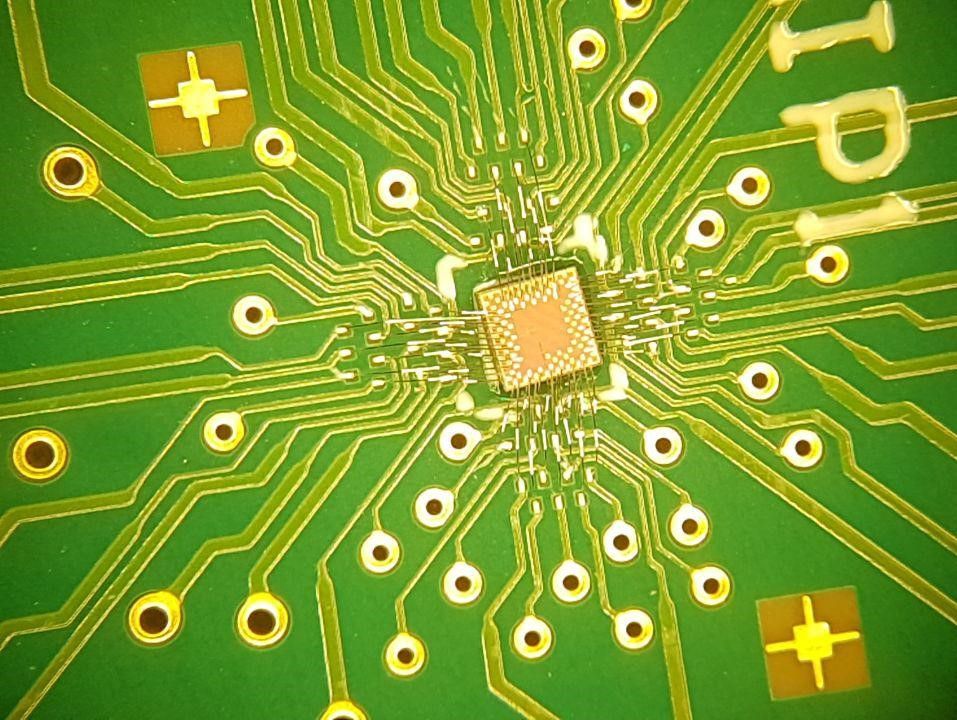
Electronic chip. Image credit: Jafar Shojaii
Explore our other research programs
Contact the Space Technology and Industry Institute
If your organisation would like to collaborate with us to solve a complex problem, or you simply want to contact our team, get in touch by calling +61 3 9214 5177 or emailing spaceinstitute@swinburne.edu.au.

